
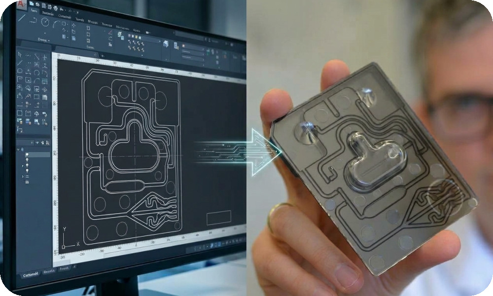
From Concept to Reality: Custom Design and Rapid Prototyping
The fundamental stage of every microfluidic project is translating abstract ideas into functional designs. At our laboratory, we bridge this gap using advanced Computer-Aided Design (CAD) software to create precise blueprints for custom microfluidic architectures. Our capabilities extend beyond the microchip itself; we simultaneously design all necessary supportive hardware, such as custom fixtures, fluidic manifolds, and sensor integration housing. Utilizing a suite of in-house rapid prototyping technologies, we rapidly convert these digital designs into physical prototypes. This integration allows for accelerated design cycles, enabling quick physical testing, functional validation, and iterative optimization before moving to full-scale fabrication.
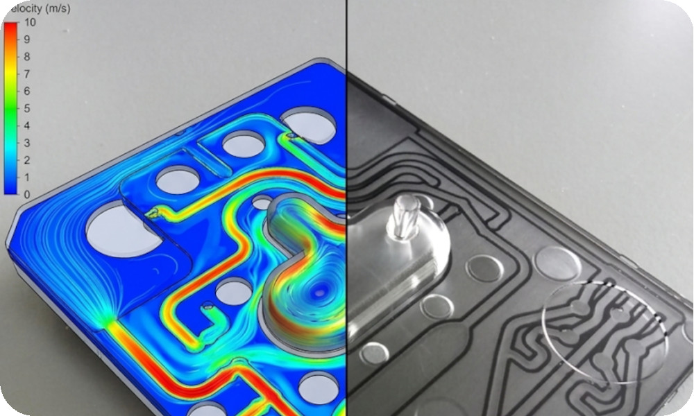
From Model to Function: Advanced CFD Simulation and Analysis
The critical phase between custom design and physical fabrication is validating the functional performance of the microfluidic architecture. We bridge this gap using high-resolution Computational Fluid Dynamics (CFD) simulation to predict the device's behavior in-silico. Our modeling capabilities go far beyond basic flow simulations. Working with the precise geometry of custom designs, we generate comprehensive maps of flow velocity and pressure profiles throughout the entire system. We then seamlessly integrate specialized physics modules, including integrated membrane transport, Lagrangian particle tracking, multi-component diffusion, and other necessary custom integrated modules. This simulation-driven strategy enables rapid verification of design rules and performance optimization. By digitally validating and refining the device’s function, we significantly reduce development risks, costs, and time-to-fabrication.
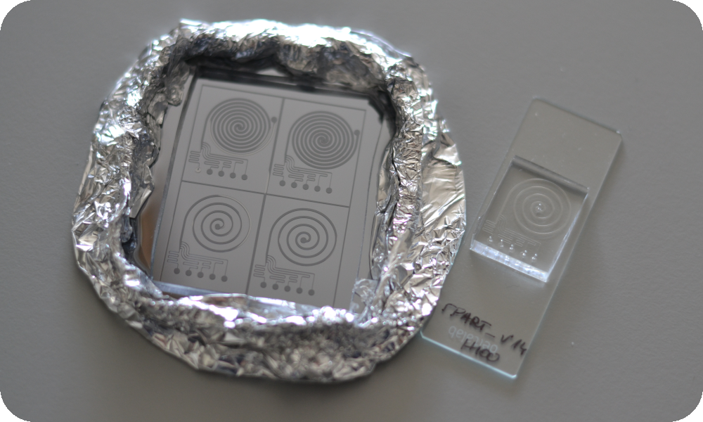
PDMS–Glass Microfluidic Chips via SU-8 Photolithography and Soft Lithography
We deliver high-precision, custom microfluidic devices using standard-setting PDMS–glass hybrid fabrication technology:
- SU-8 Photolithography: High-resolution master molds are fabricated on silicon wafers using SU-8 negative photoresist to create precise microchannel geometries.
- Soft Lithography Molding: Polydimethylsiloxane (PDMS) is cast and cured over the master mold, accurately replicating sub-micron to millimeter-scale channel features.
- Plasma Bonding: The patterned PDMS block undergoes oxygen plasma surface activation and is covalently bonded to a high-quality glass slide, forming a robust, leak-free seal.
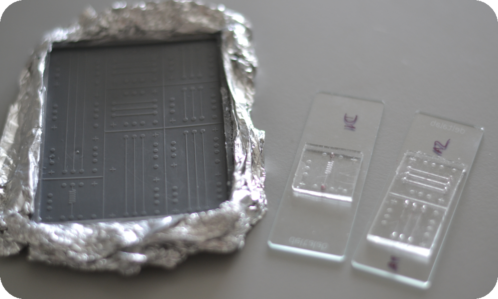
PDMS–Glass Microfluidic Chips via Stereolithography and Soft Lithography
We deliver high-precision, custom microfluidic devices leveraging additive manufacturing for rapid master mold prototyping:
- LCD Stereolithography (SLA/MSLA): Master molds are high-resolution 3D printed substrates using epoxy-based resins and LCD stereolithography.
- Soft Lithography Molding: Polydimethylsiloxane (PDMS) is cast and cured over the 3D-printed epoxy resin mold, accurately replicating microchannel networks.
- Plasma Bonding and Integration: The patterned PDMS block undergoes oxygen plasma surface activation and is covalently bonded to a high-quality glass slide, forming a robust, leak-free seal.
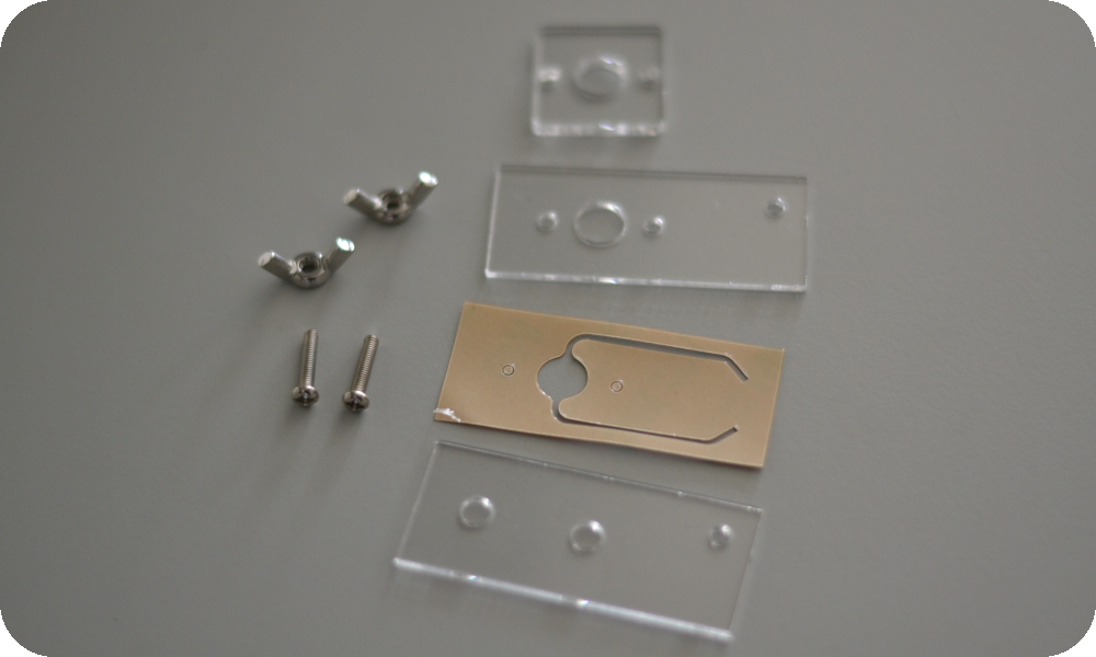
PMMA-PSA-PMMA Microfluidic Chips via Laser-Ablation and Assembly
We fabricate high-precision macrofluidic systems using laser micromachining and multi-layer bonding technologies:
- Laser Ablation and Surface Patterning: Substrates are precisely structured using high-resolution laser cutting and rastering to create intricate channels, chambers, and functional surface topologies.
- Precision Multilayer Assembly: Thermoplastic (PMMA) layers and pressure-sensitive adhesives (PSA) are aligned and stacked into robust sandwich architectures.
- Functional Membrane and Layer Integration: The modular assembly process enables seamless integration of specialized filtration membranes, electrodes, or custom functional interlayers.
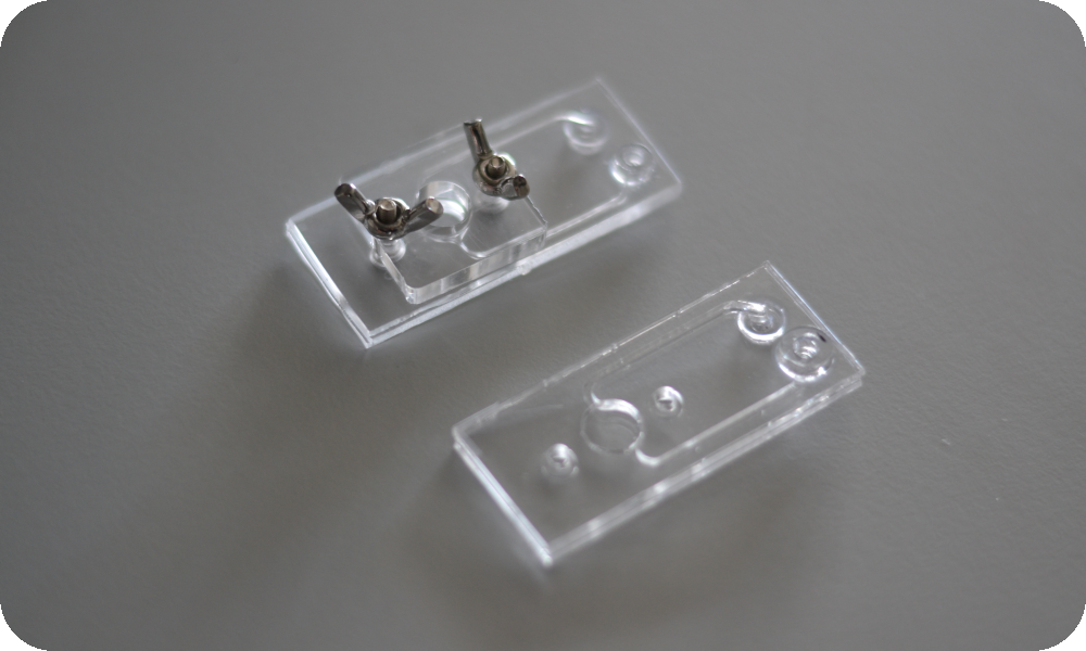
PMMA-PMMA Microfluidic Chips via Laser-Ablation and Thermal Bonding
We manufacture pure thermoplastic microfluidic systems using laser micromachining and solvent/PSA-free thermal bonding:
- Laser Ablation and Surface Patterning:PMMA substrates are precisely structured using high-resolution laser cutting and rastering to create custom fluidic systems.
- Precision Multilayer Assembly: ndividual PMMA layers are accurately stacked and aligned to form complex, multi-level sandwich architectures tailored for biological applications.
- Adhesive-Free Thermal Bonding: The aligned PMMA layers are covalently joined via direct thermal bonding, ensuring bio-inert channel surfaces and eliminating chemical leaching risks.